Digital Logic Design
Class: CSCE-312
Notes:
Lecture 2 Digital Logic Design I
Topics for today:
- #Digital signals
- #Wires
- #Transistors
- #Truth tables
- #Logic gates
- #Symbols for gates
- #Logic gates from transistors
- #Combinational circuits
- #Implementing Boolean functions with digital circuits
- #Simulating other gates with NAND
- #Computing with logic gates
- #Full adder
- #Adding two n-bit numbers with combination circuits
Digital signals
Electronic computers use Boolean logic for all computations. We need something to electrically represent 0 and 1. We use different levels of voltage, e.g. 0V and +5V. Boolean, i.e. binary, logic is used because it's easiest to have two levels instead of, say, 10.
-
It is much harder to distinguish between many different levels of voltage
-
Examples of non-electronic computers
- "Someone made a turing machine out of legos"
- Fuzzy definition but an abacus may be an analogical computer
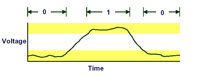
This graph shows an electric signal representing a change from 0 to 1 and back to 0.
Wires
Wires implement communication of the digital signals in the computer. Wires transport signals from one place to another. They are made of some conductive metal (i.e. copper). Although they have their limits and can be tricky, it's OK for us to think of them as being arbitrarily long, narrow, inexpensive, and fast as we build our mental model of what's going on inside the machine.
- It doesn't matter how it works at the physical level, it just matters what the interface is, put something to the wire on one end and comes out on the other end, that is it.
Transistors
"The most basic device to do electronic computations"
In a digital computer, transistors are used as the most basic element of computation. They are connected by wires. Transistors are tiny switches. They have three terminals:
- Gate (G)
- Drain (D)
- Source (S)
When the gate terminal is triggered, current is allowed to flow from the source to the drain. Otherwise, no current flows from the source to the drain, we can interpret this with a 0 and 1s states. Again, we can think of them for now as being arbitrarily small, cheap, and fast. Transistors are connected to one another and to power and ground by wires. Power and ground are concepts we don't really need for our purposes; they're just necessary for keeping the machine on. Just think of wires as pipes, like for water, that move information around, and transistors as faucets that turn the water on and off (1 and 0).
There are two types of metal-oxide semiconductor (MOS) transistors used in the CMOS (Complementary Metal Oxide Semiconductor or Complementary Mosfet) technology that dominates current computer architecture:
- NMOS - triggered (turned ON) when 1 is applied to G (gate).
			  D
	        _|
	  G --||_
	         |
	         S
-
NMOS transistors are good at passing 0's, but not good at passing 1's.
- 0s turn off the switch
-
PMOS - triggered (turned ON) when 0 is applied to G (gate).
			  D
	        _|
	  G -o||_
	         |
	         S
- PMOS transistors are good at passing 1's, but not 0's.
- 1s turn off the switch
We'll get back to transistors in a little bit.
Truth Tables
A Boolean function is a function whose domain is a vector of bits and whose range is one bit. A Boolean function can be completely described by a truth table giving the values of the function for each combination of bits in the bit vectors.
Here's a truth table for a three-input boolean function:
a b c  f(a,b,c)
0 0 0     0
0 0 1     0
0 1 0     0
0 1 1     1
1 0 0     0
1 0 1     1
1 1 0     1
1 1 1     1
- Note: you need at least two of the inputs to be 1 in order for the output of the function to be 1, this is called majority.
Logic Gates
Logic gates are physical components that implement logical functions like AND and OR. They are connected by wires to inputs, other gates, and outputs (as well as other things we will find out about later). Some important gates are:
AND, or &
	a b  a & b
	0 0    0
	0 1    0
	1 0    0
	1 1    1
- True if both the inputs are true, false otherwise
- Sometimes represented with a
*(multiply sign)
- Sometimes represented with a
OR, or |
	a b  a | b
	0 0    0
	0 1    1
	1 0    1
	1 1    1
- Sometimes represented with a
+(plus sign)
Exclusive OR, XOR, ^, or !=
	a b  a ^ b
	0 0    0
	0 1    1
	1 0    1
	1 1    0
- It's true if exactly one input is true, false otherwise
NAND
	a b  a NAND b
	0 0    1
	0 1    1
	1 0    1
	1 1    0
- The opposite of what AND would yield
- Only false if both inputs are true, otherwise it is true
NOR
	a b  a NOR b
	0 0    1
	0 1    0
	1 0    0
	1 1    0
- The opposite of what OR would yield
- Only true if both inputs are false, otherwise it is false
NOT, or ~
	a  ~a
	0   1
	1   0
- Single input function that will give the opposite of the input
Note: There are actually 16 different logic gates or functions, (24 different combinations), some of them are pretty useless.
Logic gates can have more than two inputs; what would those truth tables look like?
- They would be longer
- Example: How many rows in a truth table are there for a 4 input function?
- "How many combinations of 4 bits can you have?"
- If there are 4 inputs, the number of combinations of four things with 2 values is 24, which is 16.
- What about for 5 inputs?
- 25 = 32 rows
- For
inputs the number of rows in a truth table is
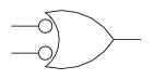
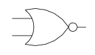
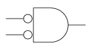
Symbols for gates
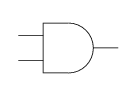
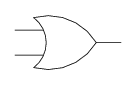
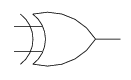
When designing a digital logic circuit, we draw a circuit diagram showing the various gates and wires connecting them. The following symbols represent logic gates:
-
AND
-
OR
-
XOR
-
NAND
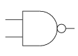
or alternately
-
NOR
or alternately
-
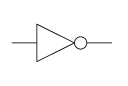
NOT
It can be very convenient to draw NAN and NOR in those alternatives to make a circuit more efficient
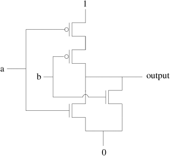
Logic gates from transistors
How do we compute with transistors? We'd like to be able to work with AND, OR, NOT, etc., not with "turn on" and "bad at passing 0."
For example, consider the NOT function:
in  out
--  ---
0    1
1    0
Here is an example of a NOT gate (or inverter) implemented with transistors:
			  1
             _|
        |-o||_
___in___|     |__out___
        |    _|
        |--||_
              |
              0
- There is a P type at the top and an N type at the bottom
- Exactly one of these transistors will turn on, the other will be off
- What if both transistors turned on?
- If both turn on we would have a problem, we would have a 0 and 1, this is a state that could be considered a bug, what would come out the output? we don't know.
- What if both transistors turned on?
How about a more complex function like NOR? Recall that the truth table for NOR is:
a  b  a NOR b
0  0    1
0  1    0
1  0    0
1  1    0
How would we implement this in transistors?
- Inputs: a, b
- If both inputs are 0 the P transistors will turn on and will let the output '1' flow
- Note: If wires that intersect are not intended to touch each other they will do a little jump over the wire.
Fact: Turns out an AND gate takes 6 transistors
- It requires more transistors than a NAND, if we instead can make computations with NAND we would gain efficiency!
Combinational Circuits
Combinational circuits are acyclic directed graphs (CSCE-221 term) whose vertices are inputs, outputs, or gates and whose edges are wires. They are drawn as circuit diagrams using the symbols we've seen. For instance, here is a combinational circuit:
- This circuit is a 2-bit adder
- It takes two 2-bit numbers, add them together and the result is a 3-bit number.
- Note: We need a 3-bit number to be able to represent the numbers 4,5, and 6.
The squares represent inputs to the circuit, while the unattached outputs represent outputs from the circuit. This circuit happens to be a 2-bit adder.
Implementing Boolean functions with digital circuits
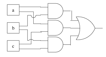
Let's look at an interesting function we might want to compute using digital logic: (majority function)
a b c  f(a,b,c)
0 0 0     0
0 0 1     0
0 1 0     0
0 1 1     1
1 0 0     0
1 0 1     1
1 1 0     1
1 1 1     1
How would we implement this function with digital logic? First, we have to figure out a formula that computes this function. How about this:
(a & b) | (b & c) | (a & c)
Yeah, that'll work. Now how do we implement this with logic gates? Like this:
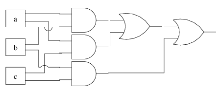
- AND and OR are associative and commutative so it is easy to combine them between inputs
Another way would be to use a 3-input OR gate:
- Think of (a')' = a
- If you 'not' two times you get the original one
Simulating other gates with NAND
It turns out that NAND is a very useful gate. A 2-input NAND consumes only 4 transistors, as opposed to AND and OR which each consume 6. Also, NAND can be used to compute any other logic function, i.e., it is complete for logic. How could we prove that?
- AND, OR, and NOT together are complete for logic, but it turns out, NAND by itself is also complete logic
- Think of inverting the output of a NAND to get the AND result, and so on.
The reasons why there are alternate symbols for NAND (as well as NOR) is because those bubbles represent NOTs that can be placed in pairs on wires to make normal ANDs and ORs into NAND (and NORs). For instance, the circuit we just saw can be drawn with just NANDs like this:
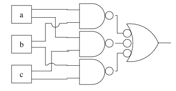
(Note that the 3-input gate is a NAND, just as an OR symbol with two bubbles on the inputs is a 2-input NAND.)
Computing with logic gates
We can use logic gates to compute with binary numbers; that's how computers do arithmetic. Imagine how you would design a circuit to do a bitwise OR, or a bitwise AND.
Majority function
Another useful function to compute would be the majority function: this function returns 1 if the majority of its inputs are 1, 0 otherwise. The function we've been with working so far is the 3-input majority function.
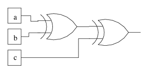
Parity function
The parity function is useful for a variety of reasons. It is true if and only if the number of inputs that are true is odd. How would you implement this function? Well, it turns out that XOR is the 2-input parity function. What about the 3-input parity function? Here's the truth table:
a b c  parity(a,b,c)
0 0 0     0
0 0 1     1
0 1 0     1
0 1 1     0
1 0 0     1
1 0 1     0
1 1 0     0
1 1 1     1
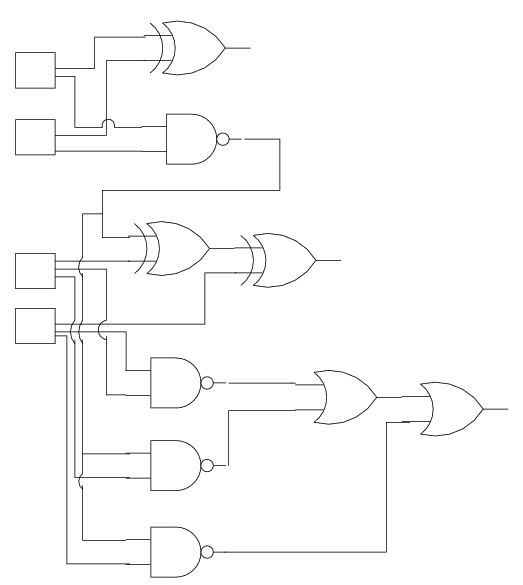
One way to implement 3-input parity is using 2 XORs, like this:
Full adder
This brings us to a more useful computation: a full adder circuit. This circuit takes as input three 1-bit numbers and produces the 2-bit sum, which can be 0, 1, 2, or 3.
Let's look at a truth table for this function:
a b c   c0 s0
0 0 0   0  0
0 0 1   0  1
0 1 0   0  1
0 1 1   1  0
1 0 0   0  1
1 0 1   1  0
1 1 0   1  0
1 1 1   1  1
c0 is the most significant bit of the sum, and s0 is the least significant bit. Notice anything? The most significant bit is the majority of the input bits, and the least significant bit is the parity. So we can build a full adder from parity and majority circuits.
Full Adder (One implementation)
/CSCE-312/Visual%20Aids/Pasted%20image%2020250913203629.png)
Adding two n-bit numbers with combination circuits
We can connect full adders to each other to form a ripple-carry adder. Let's let a full adder be represented by this symbol:
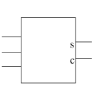
The 3 wires on the left lead from the inputs, and the wires on the right lead from the outputs with the top output being the parity (or "sum") and the bottom output being the majority (or "carry"). Then a 4-bit ripple carry adder looks like this:
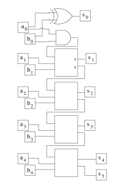
- Chunk at the top is called a half-adder
- a4 is the most significatn bit, a0 is the least significant bit
- Carry is rippling though the full adders until the end where there will be two outputs
- the result will be an n+1-bit number